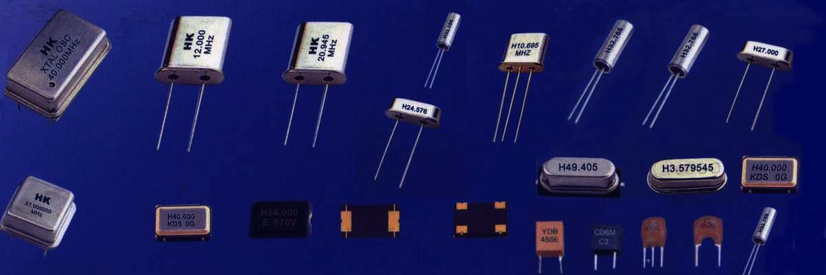
|
The circuit, as shown in Fig.5 denotes the quantities L1,C1,R6
and C0 as the electrical equivalent the electromechanical and
electrical properties of the quartz and holder assembly. L1
and C1 are referred to as the motional inductance and
capacitance
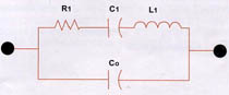 Fig.5 Equivalent Circuit
 respectively, and R1
is know as the effective series resistance (ESR).C0 is the static
or shunt capacitance whose value is the sum of the capacitance
between the electrodes and capacitances added by the leads and
holder. Equivalent
Series Resistance (ESR)
The resistive element, measured in ohms, of a crystal device.
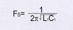
At the frequency denoted by the following formula, the motional
inductance (L1) and motional capacitance (C1)are of equal
ohmic value are exactly opposite in phase, the net result
is that they cancel one another and only a resistance remains
in the series leg of the above equivalent ciruit(Fig.5).The
ESR measurement is made only at the series resonant frequency
(Fs),not at some predetermined parallel resonant frequency
(FL). Crystal resistance measured at some parallel load resonant
frequency is often called the effective resistance.
 Overtone
Crystals
Because of physical properties and geometry of an AT cut quartz
blank, a crystal can vibrate at many frequencies. The lowest
frequency is called the fundamental frequency and can be supplied
up to about 45MHz. Higher frequencies (to over 200MHz) are
achieved
by operating the crystal oscillates at its designed overtone
frequency (Fig.6).
Overtone crystals are specially processed for plane parallelism
and surface finish in order to enhance their performance at
the required overtone frequency. The overtone frequency is higher
than the equivalent harmonic multiple of the fundamental by
approximately 25MHz per overtone.
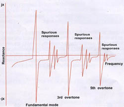 Fig.6 Overtone Response of a Quartz Crystal
Spurious Response
It is also possible for a crystal to vibrate at a frequency
that is not related to its fundamental or overtone
frequencies. Such
undesired frequencies are referred to spurious responses (Fig.6).
The manufacturing processes are designed to minimize (not eliminate)
the spurious responses and maximize the crystal activity at
the desired frequency. The circuit designer should further
guard against spurious responses by ensuring that the oscillator
feedback circuit achieves its highest gain at the desired
operating frequency.
|